Image of Intel Meteor Lake laptop processor released – fourteenth generation Core

Stephen Shankland from CNET He visited the Arizona chip factory and had a blue team, and fortunately shared the first image of Intel’s Meteor Lake laptop processor. While the tech giant has yet to unveil its twelfth-generation mobile processors, the Alder Lake P and Alder Lake M, we see these images of the next two generations of test silicones.
The images were taken at Intel’s Fab 42 plant in Chandler, Arizona. CNET has also released close-up photos of several other chips, including the next-generation Xeon Scalable with HBM memory and codenamed Sapphire Rapids or even the Ponte Vecchio data center accelerator.
Image of Intel Meteor Lake laptop processor
Most interesting of all is the image that Stephen took of the 300mm wafer of Meteor Lake M processors, fourteen-generation low-power models. In fact, these are the first images of real silicon that have actually been produced experimentally. In fact, there is one thing in common between all these chips, and that is the design of MCM with advanced packaging technologies. An issue that Intel is using to use in its new generation of products.


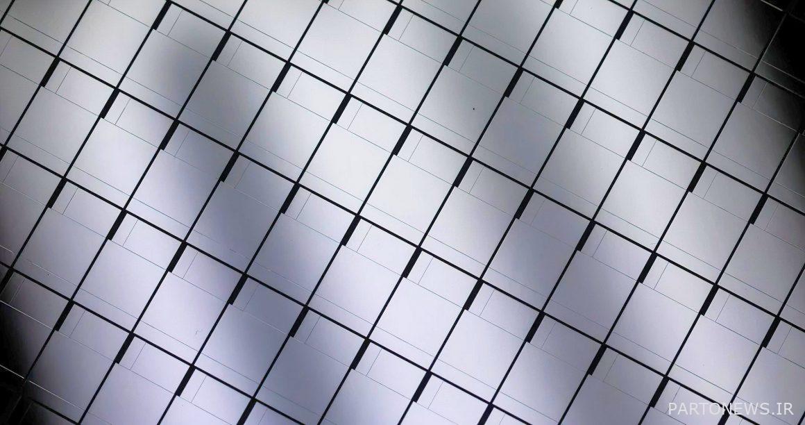
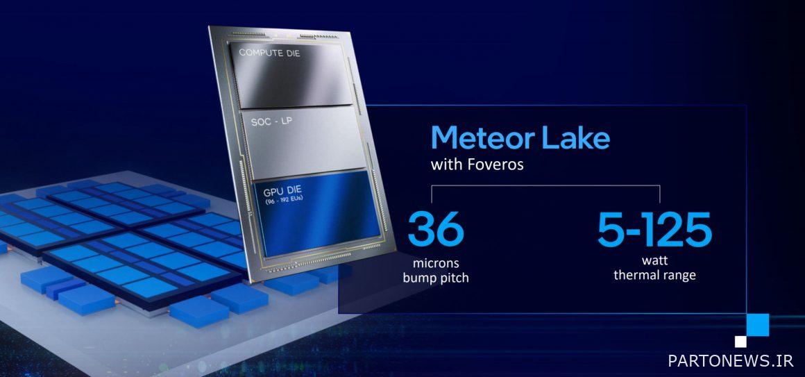
Based on the dimensions of these chips, as mentioned, we will probably see the Meteor Lake M series, which will operate in the temperature range of 5 to 15 watts. The point is, it’s unclear where each Tile or chip on the package works. Intel has confirmed that Meteor Lake will use Foveros technology, and up to three Tiles have been approved for it: Compute Die (probably the largest die in the images), SoC LP for input / output, and a graphical die that may hold 96 to 192 executables. It has a place in itself. The experimental chip, however, clearly contains four Tiles, the purpose of which is currently unknown.

| Series | Processor architecture | Manufacturing technology | Maximum number of cores | Platform chipset | Platform socket | Memory supported | thermal power | PCIe support | Release date |
| Intel Sandy Bridge | Sandy Bridge | 32 nm | 4/8 | Series 6 | LGA 1155 | DDR3 | 35 to 95 watts | PCIe Gen 2.0 | 2011 |
| Intel Ivy Bridge | Ivy Bridge | 22 nm | 4/8 | Series 7 | LGA 1155 | DDR3 | 35 to 77 watts | PCIe Gen 3.0 | 2012 |
| Intel Haswell | Haswell | 22 nm | 4/8 | Series 8 | LGA 1150 | DDR3 | 35 to 84 watts | PCIe Gen 3.0 | 2013 to 2014 |
| Intel Broadwell | Broadwell | 14 nm | 4/8 | Series 9 | LGA 1150 | DDR3 | 65 watts | PCIe Gen 3.0 | 2015 |
| Intel Skylake | Skylake | 14 nm | 4/8 | Series 100 | LGA 1151 | DDR4 / DDR3L | 35 to 91 watts | PCIe Gen 3.0 | 2015 |
| Intel Kaby Lake | Kaby Lake | 14 nm plus | 4/8 | Series 200 | LGA 1151 | DDR4 / DDR3L | 35 to 91 watts | PCIe Gen 3.0 | 2017 |
| Intel Coffee Lake | Coffee Lake | 14nm plus plus | 6/12 | Series 300 | LGA 1151 | DDR4 | 35 to 95 watts | PCIe Gen 3.0 | 2017 |
| Intel Coffee Lake Refresh | Coffee Lake | 14nm plus plus | 8/16 | Series 300 | LGA 1151 | DDR4 | 35 to 95 watts | PCIe Gen 3.0 | 2018 |
| Intel Comet Lake | Comet Lake | 14nm plus plus | 10/20 | Series 400 | LGA 1200 | DDR4 | 35 to 120 watts | PCIe Gen 3.0 | 2020 |
| Intel Rocket Lake | Rocket Lake | 14nm plus plus | 8/16 | Series 500 | LGA 1200 | DDR4 | Unknown | PCIe Gen 4.0? | 2021 |
| Intel Alder Lake | Alder Lake | Intel 7 | 16/24? | 600 series? | LGA 1700 | DDR5 | Unknown | PCIe Gen 5.0? | 2021? |
| Intel Raptor Lake | Raptor Lake | Intel 7 | 16/30? | 700 series? | LGA 1700 | DDR5 | Unknown | PCIe Gen 5.0? | 2022? |
| Intel Meteor Lake | Meteor Lake | Intel 4 | Unknown | 800 series? | LGA 1700? | DDR5? | 5 to 125 watts | PCIe Gen 5.0? | 2023? |
| Intel Arrow Lake | Arrow Lake | Intel 4? | 40/48? | 900 series? | Unknown | DDR5? | Unknown | PCIe Gen 5.0? | 2024 |
| Intel Lunar Lake | Lunar Lake | Intel 3? | Unknown | 1000 series? | Unknown | DDR5? | Unknown | PCIe Gen 5.0? | 2025? |
| Intel Nova Lake | Nova Lake | Intel 3? | Unknown | 2000 series? | Unknown | DDR5? | Unknown | PCIe Gen 6.0? | 2026? |
Score: 5.0 Out of 5 (1 vote)
wait a little…